


Tech Brief
How to Design RF Amplifiers for Space-based Acousto-optic Tunable Filter Systems
Introduction
A wide range of space-based scientific instruments (such as spectrometers) use direct observation of light—visible, ultraviolet, or infrared—to form images, to analyze the composition of atmospheric gases, or to determine the composition of rocks and soils. These sophisticated devices are composed of complex electronics, firmware, software, state-of-the-art signal processing algorithms, and a wide variety of technologies. Two key elements are critical for the overall performance of the instrument: the acousto-optic tuneable filter (AOTF) and its associated radio frequency driver (RF driver). The AOTF is a crystal that acts as an optical filter. If the crystal is excited with a specific radio frequency signal, its response is tuned to a specific wavelength. As such, the instrument can use this excitation property to dynamically select specific wavelengths with unmatched accuracy by electrically selecting the radio frequency of the driver. Designing and building an RF amplifier that can boost the low power generated RF signal to the few watts required by the crystal may appear easy to experienced RF designers, but the special conditions of the space environment and the specificities of the signal required by the AOTF make this task an interesting and singular challenge.
Amplifier Requirements
The simplified RF makeup of the subsystem consists of an RF generator followed by the RF amplifier (or RF driver) and the AOTF. The RF generator normally delivers low-output power, at around 0 dBm; the AOTF normally requires input power levels between 0.5 and 5 W. The RF source requires frequency ranges in the 1 to 500 MHz range and are unique for each AOTF type depending on the wavelength of operation. The selected frequency bandwidths are normally one-octave or multi-octave and impose an additional critical requirement to second harmonic rejection.
Another important requirement describes the power consumption of the amplifier during operation, which can also be expressed as RF power efficiency (RF output power (W) / DC Power consumed – (W)). It is normally critical in space-based platforms not only because of power consumption itself, but also because of limited options for heat dissipation inside the spacecraft. In addition, power efficiency decreases as the linearity (and second harmonic rejection) increases.
Finally, and no less important, space environments impose specific requirements for reliability and radiation tolerance, which are critical for RF transistors. This makes choosing the correct devices in the design of the amplifier even more critical.
Table 1 summarizes the key requirements for the RF amplifiers on these systems, accompanied by three practical examples of real-life applications.
| General Specification | Example 1 | Example 2 | Example 3 | |
|---|---|---|---|---|
| Instrument on the Moon’s Surface | Instrument in Mars’ Orbit | Instrument in Deep Space | ||
| Frequency Range | 1 to 500 MHz Octave and Multi-octave | 30-210 MHz | 14-30 MHz | 70-110 MHz |
| Gain | 25-40 dB | 35 dB | 38 dB | 30 dB |
| Nominal RF Output Power | 0.5 to 5 W | 3 W | 2 W | 0.5 W |
| Minimum Allowable Harmonic Rejection | As Low as Possible | -20 dBc max. | -18 dBc max. | -35 dBc max. |
| Power Consumption | As Low as Possible | < 15 W | < 6 W | < 2 W |
| Radiation (TID) | Parts Qualified Above This Level can be Used Without Restrictions | 20 Krad | 20 Krad | 20 Krad |
Table 1: General requirements for RF amplifiers and three specific examples.
The three examples listed in the table above have things in common, but the combination of frequency and power identifies critical specifications. You must critically analyze both to succeed with your design.
Transistor Selection
Selecting the correct transistor is one of the most sensitive stages of any amplifier design, but in this case it is the most critical step. The frequency range is low enough to be able to use low frequency technologies, (such as silicon RF MOS-FET) but high enough to tolerate wide bandgap semiconductors such as GaAs (transistor or MMIC). Table 2 presents different semiconductor technologies.
| Design Based in Push-Pull RF MOS-FET | Design Based in Single Ended RF MOS-FET | GaAs FET | GaAs MMIC | |
|---|---|---|---|---|
| RF Power Capability | ++ | + | ++ | ++ |
| Harmonics Rejection in Band | +++ | - | + | + |
| Power Efficiency | - | + | --- | --- |
| Radiation | - | - | +++ | +++ |
| Availability of Space Parts | - | - | ++ | + |
| Integration Simplicity | + | ++ | - | --- |
| Amplifier Price | ++ | + | - | --- |
Table 2: Trade-off transistor selection.
RF MOS-FETs are normally simple and inexpensive solutions and can be directly biased with one single external voltage (such as 12 V) and allow easy and reliable integration. They also offer enough RF power capability for this application. The in-band harmonic rejection in multi-octave designs does not perform poorly with single-ended devices and is excellent for second harmonic in push-pull configurations. On the other hand, they are silicon-based, which is sensitive to radiation even at low doses, so you must provide extra shielding or perform testing. There are few space-qualified parts, so be prepared to perform extra screening and analysis.
GaAs devices are very good in terms of RF power capability, harmonic rejection, and in general in RF performance. They are also well-suited for radiation tolerances since the technology is rated up to 300 krad and there are space-qualified parts already available in the market. However, they come with big drawbacks for this application. Most of the active GaAs devices suitable for this application need a positive drain voltage for DC bias and a negative gate voltage. In addition, at power ON and OFF, you must apply both voltages in a certain sequence so as not to damage the transistor. Consequently, a robust amplifier requires additional active circuitry (DC/DC, OP amps, regulators, and so on), making more complex and sophisticated designs. This extra circuitry affects the overall DC power consumption. MMICs add extra complexity in attaching the die and performing the wire bonding.
There are several interpretations of this trade-off depending on the rest of the parameters. However, if the radiation and lifetime of the mission are not extremely demanding and the system can count on some shielding and good EEE components assessment, then RF-MOS are an excellent and efficient choice, even for intense multi-octave designs. On the other hand, if radiation is a critical parameter in your design, and you have sufficient budget for a good design, you can create an excellent amplifier with GaAs.
We selected a MOS transistor for examples 1 and 2 due to their relatively low radiation requirement, support for the customer’s use of commercial transistors combined with screening, efficiency and simple integration approach. We selected a single-ended MOS transistor for example 2 and a push-pull for example 1 to optimize the response for their different bandwidths and RF power requirements. Example 3 requires a higher level of qualification for component selection as well as higher radiation tolerances. In this case, there was a sufficient budget and the mission had a longer duration in a more exposed environment. For those reasons, we selected a GaAs space-qualified transistor.
Tuning the Working Point
Once you have selected the transistor technology, you must select the working point. Models and software tools are always helpful, but the low frequency and low power of these designs, along with the requirement for fine tuning, suggest that you design and build simple breadboards that allow you to adjust the transistor bias points while monitoring the power consumption, the RF output power, and the rejection of the in-band harmonics.
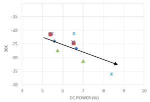
We suggest a methodology in which you first set the optimum RF output power where the amplifier must operate, and then evaluate different working points in a trade-off between harmonic rejection and DC power consumption. Using this approach, you can find the optimum RF working point for the required RF output power, which allows you to arrive at the best trade-off between consumed DC power and harmonics rejection. Figure 1 presents an example of such a trade-off, with the RF output transistor set for an output power of 2 W and different working points. Observe the clear relationship between DC power consumption (amplifier working towards a pure A class) and harmonic rejections down to -35 dBc. On the contrary, when the amplifier is driven to an AB class, you can observe lower power consumption down to 5.5 W, but you pay the price of harmonic rejections as high as -22 dBc.
These first approaches are very useful for optimizing the working point. Once you set the working point, you can build the rest of the amplifier around it, considering the rest of the parameters such as matching networks, stability, heat dissipation, mechanical design, temperature behaviour, RF gain stages, and so on. We recommend a second optimization iteration using the same concept once the amplifier is completely designed.
Figure 1: Tuning of amplifier working point for 33 dBm output power at frequency worst case.
Results
Table 3 summarizes the results of the three amplifiers, with internal pictures of the three flight models.
| General Specification | Example 1 | Example 2 | Example 3 |
|---|---|---|---|
| Instrument on the Moon’s Surface | Instrument in Mars’ Orbit | Instrument in Deep Space | |
| Frequency (MHz) | 30-210 MHz | 14-30 MHz | 70-110 MHz |
| Nominal Output Power (dBm) | 34.7 | 33 | 27 |
| Gain (dB) | 35 | 38 | 30 |
| P1dB (dBm) | 34.7 | 33 | 27 |
| Harmonics at Nominal Output Power (dBc) | -20 / -45 | -18 / 30 | -45 |
| DC Power at Nominal RF Out | < 14.5 W | < 6 W | < 1.5 W |
| RF Power Efficiency at Nominal Working Point | 20% | 33% | 33% |
| Unit Cost Efficiency | +++ | + | - |
Table 3: Final results of the three examples
Observe that the amplifier in Example 1 gives the highest output power for the widest bandwidth while offering a reasonably good harmonic response over the whole bandwidth. It also has the simplest implementation and the most efficient price. One drawback is that the unit has the highest power consumption. We implemented a dedicated cooling structure at the instrument.
The amplifier in Example 3 is by far the most complex and expensive, with two layers of electronics (only one appears in the picture). It is also the one delivering less output power and has the best harmonic response, because its bandwidth is less than one octave. It is also the one able to tolerate higher radiation doses.
Finally, the amplifier in Example 2 is half-way between both, with an octave bandwidth, offering a compromise in terms of power efficiency, harmonic rejection, and output power level. In terms of complexity, it is similar to Example 1 although is more compressed due to limited available space.
Conclusion
This document analyses the design methodology of RF amplifiers that work with AOTFs in space-based instruments. The critical parameters and specifications imposed by the instrument on the RF amplifier requires a unique approach in the design and manufacture of such devices. Selecting the correct transistor is critical; you can use different technologies depending on the final instrument configuration. Dedicated test benches are highly useful in performing DC-harmonic sweeps at an early design stage to achieve the optimum design. Finally, it presents three different implementation examples of amplifiers working on space instruments, highlighting how the same design methodology has been successfully applied to three different designs.
Next Steps
ERZIA has broad experience designing complex RF and microwave amplifiers from low frequency to 100 GHz for demanding environments such as space, aeronautics, and defense. Check our www.erzia.com for a list of existing COTS or request a custom design.
References
- NOMAD spectrometer on the ExoMars trace gas orbiter mission: part 1—design, manufacturing and testing of the infrared channels
- Operating principles and detection characteristics of the Visible and Near-Infrared Imaging Spectrometer in the Chang’e-3
- Visible and near-infrared imaging spectrometer and its preliminary results from the Chang’E 3 project
- Laser modulator for LISA pathfinder